
BatchDrake
Hacking, HAM Radio (EA1IYR), DSP, physics and more
Hacking, HAM Radio (EA1IYR), DSP, physics and more
Years ago (2008?), in the middle of an outburst of interest in electronics, I decided to dismantle my aunt’s old VHS recorder, a Sanyo VHR 7100EE, which she replaced by a generic uninteresting DVD player days earlier.
It was not the first time I disassembled a VCR. I did it multiple times in the past for minor repairments (like a worn out pinch roller that wrinkled the tapes), but back then I wanted to go a bit further. I extracted the main PCB, the head drum, the power supply and a couple of things more, being the 24-pin VFD display the only piece that remained with me until today.
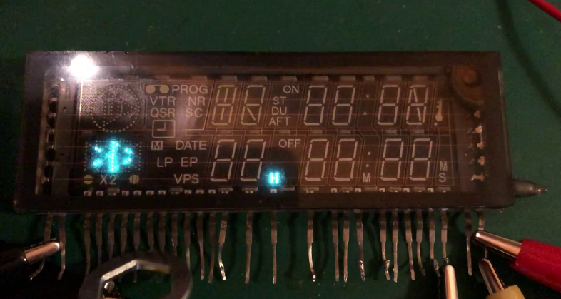 Testing the VFD after more than 10 years.
VFD displays are particular cases of warm cathode vacuum tubes, in which (usually) 7-segment-shaped anodes are coted with a phosphorescent substance that light up when they are hit by an electron flow coming out of the heated filament due to thermionic emission (also called Edison effect).
The anodes are conditionally polarized at a relatively high voltage (25V is a typical value), depending on the segment to light up. A third element (the grid) is placed between the filament and the anodes which, when positively polarized, let electrons flow from the filaments to the anodes. If the grid is negatively polarized, electrons remain in the surroundings of the filament and never reach the anode.
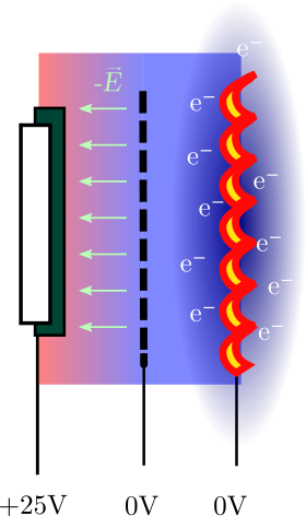 | 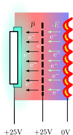 |
| Filament (cathode) and anode in direct polarization. Negatively-polarized gris produces a plateau in the potential field which prevents thermal electrons from leaving the filament. | When the grid is positively polarized, the potential field around the filament turns into a slope along which electrons slide down to the grid, acquiring kinetic energy (i.e. linear momentum). The plateau between the grid and the anode leaves their momentum untouched, and electrons just hit the phosphorescent coating with their recently acquired velocity, producing light. |
Filaments must be powered with a relatively low-voltage (around 6V, depending on the specific VFD), high enough to produce thermal emission, low enough to the prevent filaments from visually glowing. This is something important to take into account when dealing with this kind of tubes: if your filament glows in visible light, you are damaging it. The ability of the filament to release thermal electrons is possible thanks to a special coating that wears out with usage. The higher the filament temperature is, the faster it wears out.
In this display, filament terminals were in both sides of the display, exposing 2 shorted pins for each terminal. The appropriate voltage for the filament was determined experimentally: a little less than 4V was enough to produce thermal emission without making the filaments glow. Since I planned to power my circuit with the typical TTL voltage of 5V and the filament resistance was measured to be 30Ω, I could just simply make a simple voltage divider by placing a resistor in series with the filament to get the desired drop of 4V:
\[\frac{30\Omega}{30\Omega+R_s}=\frac{4\text{V}}{5\text{V}}\implies R_s=7.5\Omega\]Since I didn’t have any 7.5Ω resistor around, I had to settle for a parallel association of two resistors of 10Ω and 33Ω, giving an equivalent resistance of 7.6Ω. Good enough!
It is also recommended to power the filaments with AC instead of DC, although this is (in principle) needed for aspectual reasons: if the filaments are powered with DC, a circular magnetic field is produced around them, causing the flow of electrons to divert as they travel through the gap between the filament and the anodes. The result is a segment that glows irregularly, due to the differences in the density of the electron flow caused by the magnetic fields. AC currents keep these magnetic fields oscillating, compensating the irregularities along a cycle.
Unfortunately, the only power supply I had in reach was a regulable DC power supply, so I had to settle for irregularly illuminated segments. Results were not that bad after all.
A pin-by-pin test of the display let me conclude that 9 pins controlled the grids, while the remaining 15 controlled the specific segment within the selected grid. Multiple anodes in different grids were wired together, implying that if I want to display different numbers in the VFD I have to cycle through all 9 grids fast, setting the segment pins for each grid accordingly. This inspired me to make a simple VFD controller, based on an old STM32VLNDISCOVERY board I acquired back in college.
The problem with this VFD was that, since the voltages were that high, the TTL levels (3,3V-0V) I could get out of the STM board pins were simply not enough. I needed to design some kind of interface circuit to switch the segments on and off with . That’s when I came across the ULN2803A, an IC consisting of an array of 8 NPN Darlington transistors, that can be used as a simple low-voltage-driven switch. These ICs ara rather inexpensive (0.70 USD in DigitSpace) and are therefore ideal for hobbyist experiments. Since every ULN2803A has 8 transistors, and I need to conver the voltages of 24 pins, 3 ULN2803As will be required.
A Darlington pair is a two BJT transistor association in which the first transistor is cascaded to the second, acting as a single transistor with high current gain (around the product of both). This means that it is also possible to saturate the pair with a smaller IB than with a single transistor.
 Typical Darlington configuration of two NPN/PNP transistors. Pure NPN / PNP configurations are also possible.
The ULN2803A’s equivalent circuit for each input is, however, slightly more complicated:
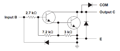 The ULN2803A equivalent circuit. Note the NPN-NPN configuration.
The 2.7K resistor limits the base current when the input is raised to a high TTL level (around 1mA at 3.85V in the input). When the input is high the pair saturates and acts effectively as a short circuit (i.e. switched on). Conversely, when the input is low, the pair is in the cutoff region, acting as an open circuit (i.e, switched off).
The resulting interface circuit will be as simple as a Darlington pair with a pull-up resistor for each VFD pin. When the input is low, the pair is in cut-off state, no current flows from collector to emitter and the pull-up resistor raises the output to 25 V, with no dissipation. Setting the input to high (3.3V) will saturate the pair, making it act as a short circuit, setting the output to a low voltage and turning the corresponding segment/grid off. The pull-up resistor will be dissipating in order to keep the voltage difference in its terminals, letting a 2.5 mA current pass through the transistor:
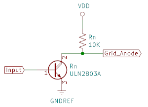
Note that this interfacing circuit makes the VFD work in reverse logic, which may make you think “but… hey, you will have at least 8 grids off everytime, your circuit will be dissipating most of the time!”. And you would be totally right. However, I did it on purpose for two reasons: a) I planned to use another TTL IC to turn the grids on and off, which happened to work in reverse logic too and b) I also wanted to see everything incrementally glowing as I soldered every pin one by one, so I could see if I miswired something in the process.
Since 24 pins are a lot, 9 of them belonging to the grids (of which only one is in high level every time), I thought I could save some outputs of the STM32 if I used 4 pins of them to encode the grid number, instead of using 9 outputs to turn each grid on and off. This can be achived by plugging 8 of the Darlington grid inputs to the output of a 74LS138N 3-to-8 decoder, saving 5 wires. Since I need at least 4 bits to encode a number from 1 to 9 (or 0 to 8), I can wire the most significant bit input to both the 9th grid input and the strobe input of the decoder. This way, if the MSB is 0, the 74LS138N is disabled while the 9th grid is on, and vice-versa. Of course I would have to negate the MSB of the grid number, but that’s something I can do programatically.
Finally, in order to obtain 25V from a 5V power supply, I took the path of least resistance and acquired a MT3608 DC boost converter, which can produce 25V out of 5V easily.
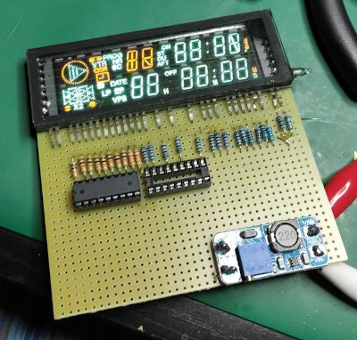
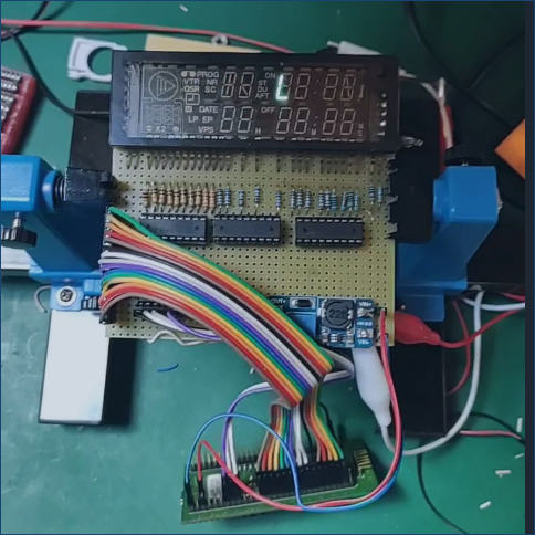
I used a spare prototyping board I bought some years ago for projects like this. Since this was my first DIY electronics project in many years, I didn’t want to risk the ICs by applying too much heat with the solderer. Sockets are a good investment here: apart from keeping me from damaging the ICs, reusing the ICs for future projects is as simple as unplugging them from the sockets.
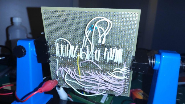
 All 10K pull-up resistors soldered to the 24 grid/anode pins. The 10Ω and 33Ω resistors on the right are connected in series with the filament and in parallel with respect to each other, dropping 1V of the supply voltage.
It was the first time I wired a prototyping board, and it was challenging at first because of the proximity of the connections. On the other hand, it made myself confident with my solderer. It looks messy, but hey, ancient computers were way worse than this:
The complete circuit includes the three ULN2803A connected to the 24 pins of the VFD. The extra IC on the bottom-left is the 74LS138N used to decode the grid number:
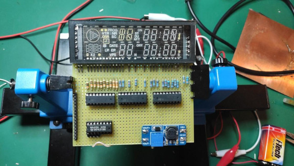
The TTL segment inputs in the left an the 4-bit grid number inputs below the decoder were cut out from a basic 40 pin row. These pins were then connected to the STM GPIO pins using female-to-female DuPont cables. The STM was powered by wiring its Vcc and GND pins to the boost converter 5V input:
And finally, after experimentally identifying GPIO outputs with each segment / grid bit, I wrote a small C program for the STM that implemented the logic to cycle around grids and set the segments on and off. The program is highly dependant on my wiring and it is barely portable, but I include it here for the sake of completeness:
#include "stm32f10x.h"

#define DELAY_LENGTH 30

#define VFD_GRID_NUM 9

#define VFD_SEG(x) (1 << (x))

#define VFD_SEG_1_EXTRA   VFD_SEG(6)
#define VFD_SEG_1_CENTER  VFD_SEG(7)
#define VFD_SEG_1_DOWN    VFD_SEG(9)
#define VFD_SEG_1_DNLEFT  VFD_SEG(10)
#define VFD_SEG_1_UPLEFT  VFD_SEG(11)
#define VFD_SEG_1_DNRIGHT VFD_SEG(12)
#define VFD_SEG_1_UPRIGHT VFD_SEG(13)
#define VFD_SEG_1_UP      VFD_SEG(14)
#define VFD_SEG_1_ALL     0x7e80

#define VFD_SEG_2_CENTER  VFD_SEG(0)
#define VFD_SEG_2_UPLEFT  VFD_SEG(1)
#define VFD_SEG_2_DNLEFT  VFD_SEG(2)
#define VFD_SEG_2_DOWN    VFD_SEG(3)
#define VFD_SEG_2_DNRIGHT VFD_SEG(4)
#define VFD_SEG_2_UPRIGHT VFD_SEG(5)
#define VFD_SEG_2_UP      VFD_SEG(8)
#define VFD_SEG_2_ALL     0x013f

uint16_t grids[VFD_GRID_NUM];

/* User defined function prototypes */
void init_gpio_wiring(void);
void led_toggle(void);

uint16_t
digit_to_mask(int row, unsigned c)
{
  uint16_t digits_0[10] = {
      VFD_SEG_1_ALL & ~VFD_SEG_1_CENTER,
      VFD_SEG_1_UPRIGHT | VFD_SEG_1_DNRIGHT,
      VFD_SEG_1_ALL & ~(VFD_SEG_1_UPLEFT | VFD_SEG_1_DNRIGHT),
      VFD_SEG_1_ALL & ~(VFD_SEG_1_UPLEFT | VFD_SEG_1_DNLEFT),
      VFD_SEG_1_CENTER | VFD_SEG_1_UPRIGHT | VFD_SEG_1_UPLEFT | VFD_SEG_1_DNRIGHT,
      VFD_SEG_1_ALL & ~(VFD_SEG_1_UPRIGHT | VFD_SEG_1_DNLEFT),
      VFD_SEG_1_ALL & ~VFD_SEG_1_UPRIGHT,
      VFD_SEG_1_UPRIGHT | VFD_SEG_1_DNRIGHT | VFD_SEG_1_UP | VFD_SEG_1_UPLEFT,
      VFD_SEG_1_ALL,
      VFD_SEG_1_ALL & ~VFD_SEG_1_DNLEFT
  };

  uint16_t digits_1[10] = {
      VFD_SEG_2_ALL & ~VFD_SEG_2_CENTER,
      VFD_SEG_2_UPRIGHT | VFD_SEG_2_DNRIGHT,
      VFD_SEG_2_ALL & ~(VFD_SEG_2_UPLEFT | VFD_SEG_2_DNRIGHT),
      VFD_SEG_2_ALL & ~(VFD_SEG_2_UPLEFT | VFD_SEG_2_DNLEFT),
      VFD_SEG_2_CENTER | VFD_SEG_2_UPRIGHT | VFD_SEG_2_UPLEFT | VFD_SEG_2_DNRIGHT,
      VFD_SEG_2_ALL & ~(VFD_SEG_2_UPRIGHT | VFD_SEG_2_DNLEFT),
      VFD_SEG_2_ALL & ~VFD_SEG_2_UPRIGHT,
      VFD_SEG_2_UPRIGHT | VFD_SEG_2_DNRIGHT | VFD_SEG_2_UP | VFD_SEG_2_UPLEFT,
      VFD_SEG_2_ALL,
      VFD_SEG_2_ALL & ~VFD_SEG_2_DNLEFT
  };

  if (c > 9)
    return 0;

  return row == 0 ? digits_0[c] : digits_1[c];
}

void
set_number(int row, unsigned int number)
{
  int i;

  for (i = 2; i < 8; ++i)
    grids[i] &= row == 0 ? VFD_SEG_2_ALL : VFD_SEG_1_ALL;

  if (number == 0) {
    grids[7] = digit_to_mask(row, 0);
  } else {
    i = 7;
    while (number > 0) {
      grids[i--] |= digit_to_mask(row, number % 10);
      number /= 10;

      if (i < 2)
        return;
    }
  }
}

/***********************************************
 * Initialize GPIOA PIN8 as push-pull output
 ***********************************************/
void
init_gpio_wiring(void)
{

  /*
   *  Grid outputs: PB4-PB7
   *  Segment outputs: PC6-PC9, PA8-PA15, PC10-PC12
   */
  GPIO_InitTypeDef all_gpio = {
    0xffff,
    GPIO_Speed_2MHz,
    GPIO_Mode_Out_PP };

  /* Enable PORT A clock */
  RCC_APB2PeriphClockCmd(RCC_APB2Periph_GPIOA, ENABLE);
  RCC_APB2PeriphClockCmd(RCC_APB2Periph_GPIOB, ENABLE);
  RCC_APB2PeriphClockCmd(RCC_APB2Periph_GPIOC, ENABLE);

  /* Initialize GPIOA: 50MHz, PIN8, Push-pull Output */
  GPIO_Init(GPIOA, &all_gpio);
  GPIO_Init(GPIOB, &all_gpio);
  GPIO_Init(GPIOC, &all_gpio);

  /* Turn everything off */
  GPIO_ResetBits(GPIOA, 0xffff);
  GPIO_ResetBits(GPIOB, 0xffff);
  GPIO_ResetBits(GPIOC, 0xffff);
}

void
write_segments(uint16_t segs)
{
  uint16_t seg1, seg2, seg3, seg4;

  segs = ~segs;

  seg1 = segs & 0xf;
  seg2 = (segs >> 4) & 0x1f;
  seg4 = (segs >> 9) & 7;
  seg3 = (segs >> 12) & 7;


  GPIO_Write(GPIOC, (seg1 << 6) | (seg3 << 10));
  GPIO_Write(GPIOA, (seg2 << 8) | seg4);
}

void
enable_grid(unsigned int num)
{
  uint8_t mask = 0;
  uint8_t odd = (num & 1);
  /* Grid numbers are from 0 to 8. */

  mask = (0xf0 & ~(num << 4)) ^ 0x70;
  mask |= (odd << 3) | (!odd << 8) | (odd << 9) | (odd) | (odd << 1) | (odd << 2);

  GPIO_Write(GPIOB, mask);
}

/*******************************************
 * Toggle LED
 *******************************************/
void
led_toggle(void)
{
  /* Read LED output (GPIOA PIN8) status */
  uint8_t led_bit = GPIO_ReadOutputDataBit(GPIOC, GPIO_Pin_8);

  /* If LED output set, clear it */
  if (led_bit == (uint8_t)Bit_SET)
  {
    GPIO_ResetBits(GPIOC, GPIO_Pin_8);
  }
  /* If LED output clear, set it */
  else
  {
    GPIO_SetBits(GPIOC, GPIO_Pin_8);
  }
}


void
delay(void)
{
  unsigned int i;
  static int count;

  for (i = 0; i < DELAY_LENGTH; ++i)
    ++count;
}

int
main(void)
{
  unsigned int i = 0, j = 0;

  init_gpio_wiring();

  for (;;) {
    delay();

    enable_grid(i / 10);

    write_segments(grids[i++ / 10]);

    if (i == 90) {
      i = 0;
      set_number(0, j);
      set_number(1, 999999 - j);
    }

    ++j;
  }
}
The program above displayed two counters in both rows of the VFD. This is what it looks like when running:
You may notice a bit of residual light on the left. This artifact is a consequence of two poor decisions I made:
The filament was heated by applying 0V from GND in the left and 4V from the divider in the right. This caused a voltage gradient from 0 to 4V along the filaments. The “low” level of the turned-off grids was actually the 0.7V of the VCE from the BJTs in saturation state. This 0.7V difference from the filament and the grid is enough to let some electrons slide from the filament to the polarized anodes. As you move to the right, the filament voltage increases, the grid-filament polarization reverses completely (becoming -3.8V in the rightmost grids) and the thermal electrons get repelled from them.
The results were far from perfect, but honestly, I’m glad I made these mistakes: if I didn’t connect the filament directly to the GND, I would not have had these artifacts and I would not need to look into the operation of the circuit and figure out what was going wrong.
This experiment was made possible thanks to the sponsorship of DigitSpace. Check it out!